James Madison University, Fall 2021 Semester
Lab02: Logisim ripple carry adder
Background
At a low level of abstraction, computer hardware consists of billions of
digital logic circuits. For example, memory chips are loaded with flip flops,
and CPUs have clocks, counters, adders, and so forth. In this week's lab you will
design your own circuit from scratch that will add two 4-bit integers. You can
read more about these circuits in Appendix B of the textbook and the
![]() Wikipedia article on Adders.
Wikipedia article on Adders.
Credit: This activity is based on Lab 5: Circuit design & simulation from CS 350, Spring 2012. Thank you Dr. Kirkpatrick!
Objectives
- Explain how data are represented, stored, and manipulated by computer hardware.
- Use abstraction and decomposition when reasoning about complex systems and problems.
Instructions
Notice how each circuit you design is used as an abstract tool to design a larger, more interesting circuit. If you repeat this process many many many times, you might end up with some of the computer hardware found in your laptop or smart phone!
-
First you need to install Logisim on your compuuter Logisim Free Software Note you may need to install Java, which is also free and can be found at java.com. First install try installing logisim to check if you need java. It is important you install logisim as soon as possible. You may have questions with the installation and will need help during TA hours or before Wednesday.
-
If you haven't already, work through the 5-step beginner's tutorial for Logisim. (You were expected to have completed this step before coming to the lab today.)
-
Download
 Lab02-Worksheet.txt and rename by adding your name or eid,
and read through the questions so you know what's coming. Then run Logisim.
Lab02-Worksheet.txt and rename by adding your name or eid,
and read through the questions so you know what's coming. Then run Logisim. -
Many circuits are created from smaller circuits, also called sub-circuits. To add a sub-circuit, right-click on the project name (default is Untitled) and select "Add Circuit..." Build a "Half Adder" sub-circuit that includes the following elements. Make sure you set the "Label" property of each pin to its given name, rather than adding text comments directly to the diagram.
Create two input pins named x and y.
Create two output pins named sum and carry.
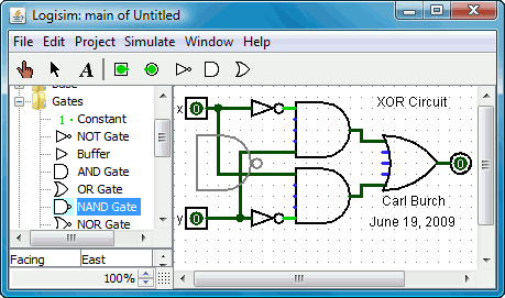
sum = x XOR y
carry = x AND y -
Using the poke tool (the finger button on the toolbar), experiment with different values of x and y to see your circuit in action. Then answer the first question in the lab worksheet.
-
At this point, you may want to save your project (name it Lab02). It's always good to save whatever files you're working on before you get too far into things. Then you can just hit Ctrl-S every 5 minutes or so, and even if the power goes out you won't lose much work.
-
Use the half adder to build a "Full Adder" sub-circuit. Like before, right-click the project and select "Add Circuit..." Once you have an empty diagram, single click once on your half adder and drop it onto the design. Complete the full adder as follows:
There are two half-adders and an OR gate.
The inputs to HA1 are pins labeled x and y.
The x input bit for HA2 is a third pin labeled carry_in.
The sum bit from HA1 is used as the y input bit for HA2.
The carry bits from HA1 and HA2 are fed into the OR gate.
Create two output pins named sum and carry_out.
The sum bit from HA2 is the sum for the full adder.
The result of the OR is the carry_out for the full adder. -
Using the poke tool, experiment with different values of x, y, and carry_in to see your circuit in action. Then answer the second question in the lab worksheet.
-
Don't forget to save your work! Remember, Ctrl-S is the keyboard shortcut for "File > Save" in most programs.
-
Use the full adder to build a 4-bit "ripple carry adder." This will be our main circuit today. (Double click "main" to design this last circuit.)
- Create two input pins labeled A and B. Change their "Data Bits" to 4. Arrange them side by side, leaving room for 4 full adders below them.
- Open the "Wiring" folder and pull out two splitters. For each, change "Fan Out" and "Bit Width In" to 4. Make both splitters face South.
- Connect each input pin to a splitter. Everything should be lined up across the top of the diagram.
- Add four full adders to your diagram. Change their "Facing" property so that the input pins are on top.
-
Now is a good time to review the diagram in Appendix B of the textbook and/or the Wikipedia article (see "Background" section above).
- Connect each pair of bits (A3+B3, A2+B2, A1+B1, A0+B0) to the x and y pins of a corresponding full adder.
- Going from right to left (least significant to most), connect the carry_out pin of one full adder to the carry_in pin of the next.
- Create a new output pin called error, and connect the carry_out of the last (most significant) full adder to it.
- Create another output pin called sum. Change its "Data Bits" to 4. Connect it to a splitter, and wire the full adder outputs to it.
- Finally, connect the carry_in of the least significant full adder to "Ground" (available in the "Wiring" folder).
-
At this point, you should feel pretty amazed at what you've done! Make sure your circuit works correctly by testing the following examples (i.e., using the poke tool).
0001 + 0001 = 0010, error=0 (i.e., 1 + 1 = 2)
0101 + 1010 = 1111, error=0 (i.e., 5 + 10 = 15)
1000 + 1000 = 0000, error=1 (i.e., 8 + 8 = 0) -
For each of your three circuits (main, full adder, half adder), export a png file. Click "File > Export Image...", uncheck the "Printer View" box, and click OK. Your file names must be main.png, full.png, and half.png. You don't need to write your name in these files.
-
Submit all three png files along with your completed lab worksheet which must be plain text file with the .txt extension, e.g., simmonsjLab2.txt, via
 canvas.jmu.edu by noon on Friday.